Transmission Electron Microscope (TEM)
- Home
- /
- Working Domain
- /
- Advanced Material Research and...
- /
- Transmission Electron Microscope (TEM)
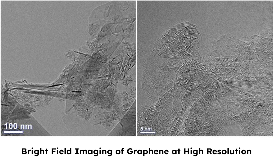
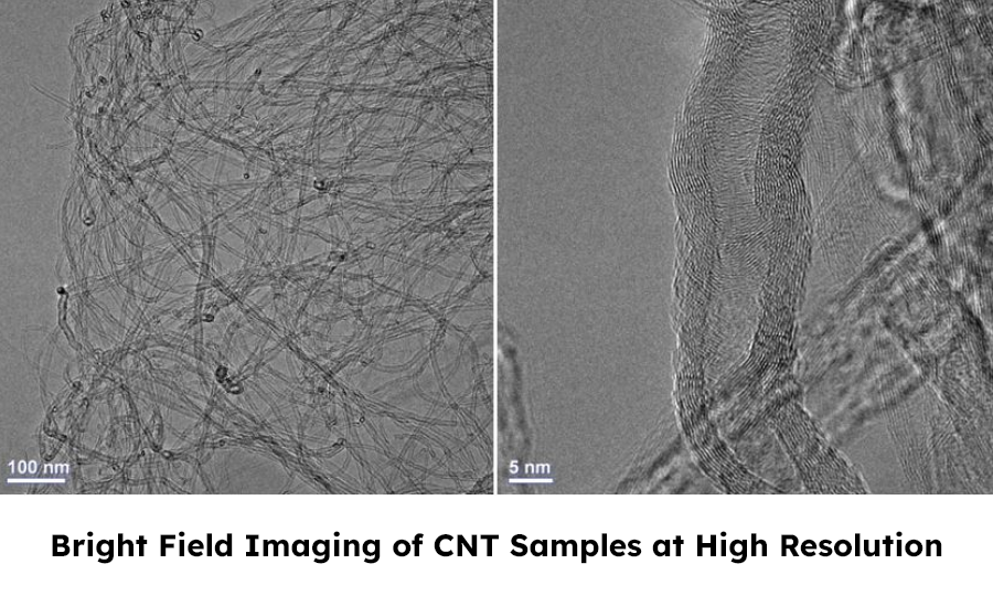
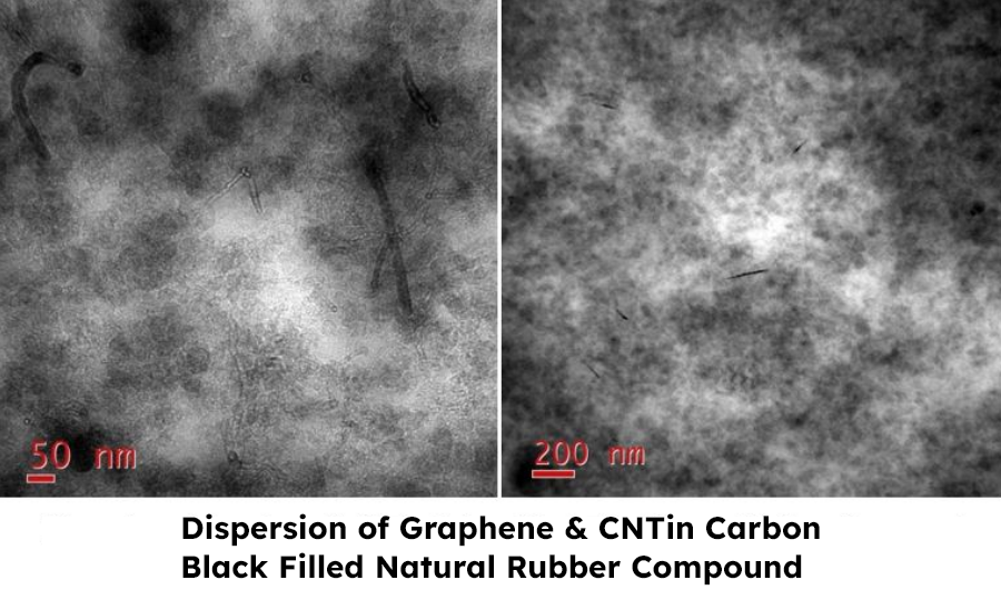
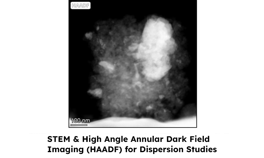
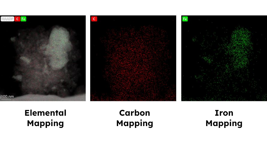
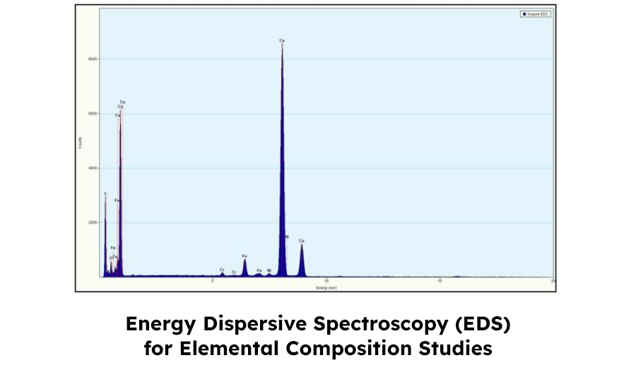
To understand the surface morphology and elemental composition of rubber compounds, HASETRI offers most precise, quantitative characterization of nanomaterials/ composites in multiple dimensions by using TEM. Information such as particle size, shape, surface morphology, topography, dispersion, quality, composition, arrangement and crystal nature can be extracted from TEM - facilitated with EDS, STEM, Elemental Mapping and Tomography.
Atomic arrangement and elemental composition of any compound is an essential criterion to understand / to obtain desired properties of it. Various physical and chemical properties such as Durability, Hardness, Rebound resilience, impermeability and adhesiveness etc., are resultant of material dispersion and composition. Hence, TEM will provide both Qualitative and Quantitative understanding of material behaviour and product performance.
It is possible to perform material studies through various modes available in TEM:
- Bright Field Imaging
- Dark Field Imaging
- High Angle Annular Dark Field imaging
- Individual element Mapping with Auto Drift
- Region specific Mapping
- Point Mapping
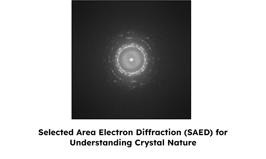
- Selected Area Electron Diffraction(SAED)
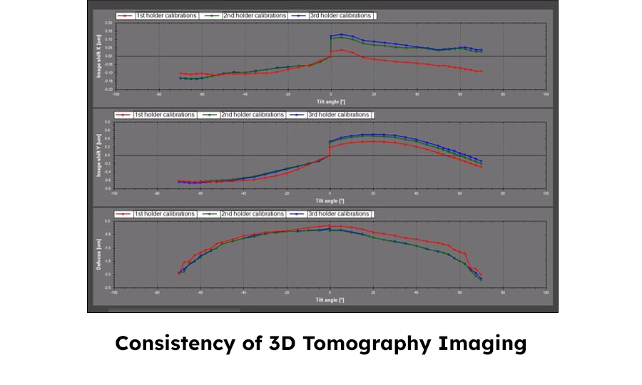
- 2D and 3D Tomography
- Scanning Transmission Electron Microscopy
- Energy Dispersive Spectroscopy (EDS)
TEM Applications
- A Transmission Electron Microscope is ideal for a number of different fields such as life sciences, nanotechnology, medical, biological and material research, forensic analysis, gemology and metallurgy as well as industry and education.
- TEM provides topographical, morphological, compositional and crystalline information.
- The images allow researchers to view samples on a molecular level, making it possible to analyse structure and texture. This information is useful in the study of crystals and metals and also has industrial applications.
- TEM can be used in semiconductor analysis and production & manufacturing of computer and silicon chips.
- Technology companies use TEMs to identify flaws, fractures and damages to micro-sized objects; this data can help fix problems and/or help to make a more durable, efficient product.
Highlights
HASETRI featured in Indian/International Rubber Journal
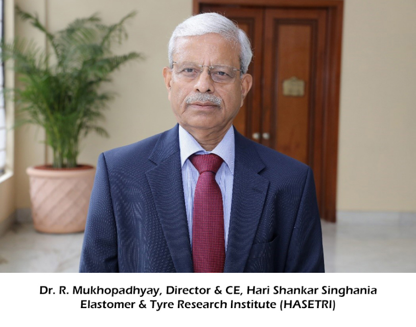
An enlightening interview with Dr. R. Mukhopadhyay, Director & CE, HASETRI, speaks of the current situation of the Indian tire and rubber industry and how they are coping with the pandemic.

HASETRI successfully enhanced the scope of NABL accreditation
September 2021: HASETRI has successfully enhanced the scope of NABL accreditation in Wet Grip and Coast by Noise testing for Cl & C2 category tyres as per ECE R117 and proposed AIS 142.
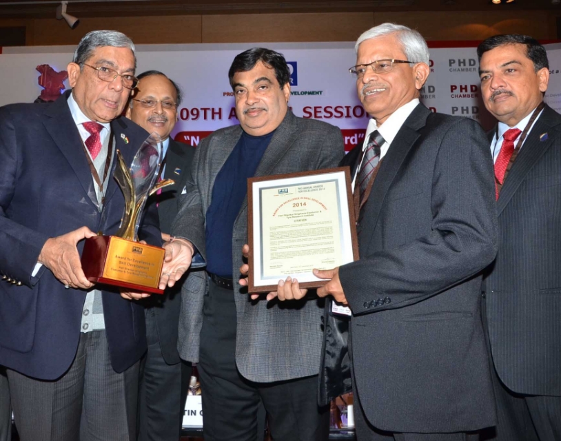
PHD Annual Awards for Excellence Announced
HASETRI imparted training to candidates under the STAR scheme of NSDC,GOI in rubber sector(under Rubber SDC)for the job roles of mill & Tyre Building Operator-commercial vehicles. The Institute has been approved as the first training provider for rubber sector by RSDC under NSDC,GOI
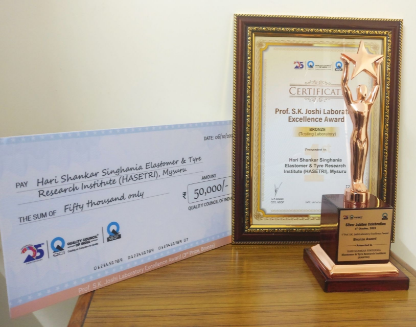
HASETRI receives the Prof. SK Joshi Laboratory Excellence Award
HASETRI received Prof. SK Joshi Laboratory Excellence Award from Quality Council of India (QCI) during their Silver Jubilee celebration held on 6th October 2022 at New Delhi. This is the first testing laboratory in private sector in India to receive this Award.
Elastomer And Tyre Research Institute